The usage of 3D circuitry is essential in persevering with to miniaturize electronics, but it surely’s been topic to severe drawbacks. The requirement for help supplies and exterior stress limits how small producers can go, however one analysis crew may need a solution. The engineers have developed a method to construct free-standing, self-healing metallic buildings with out these wants.
Led by Affiliate Professor Benjamin Tee, the analysis crew from the Nationwide College of Singapore (NUS) lately printed its findings. Calling its expertise CHARM3D, the crew demonstrated the way it can use 3D metallic printing expertise to manufacture a variety of compact electronics, together with wearable sensors, wi-fi communication methods, and electromagnetic metamaterials.
NUS researchers develop a novel approach to manufacture 3D circuits for superior electronics – YouTube
Watch On
One use the crew has recognized for its expertise is in healthcare. Tee and his crew say that CHARM3D permits for the event of important signal monitoring units which might be fully non-contact. The affected person simply positions themselves close to the sensor, which may detect respiratory and different important indicators with out ever touching the affected person’s pores and skin.
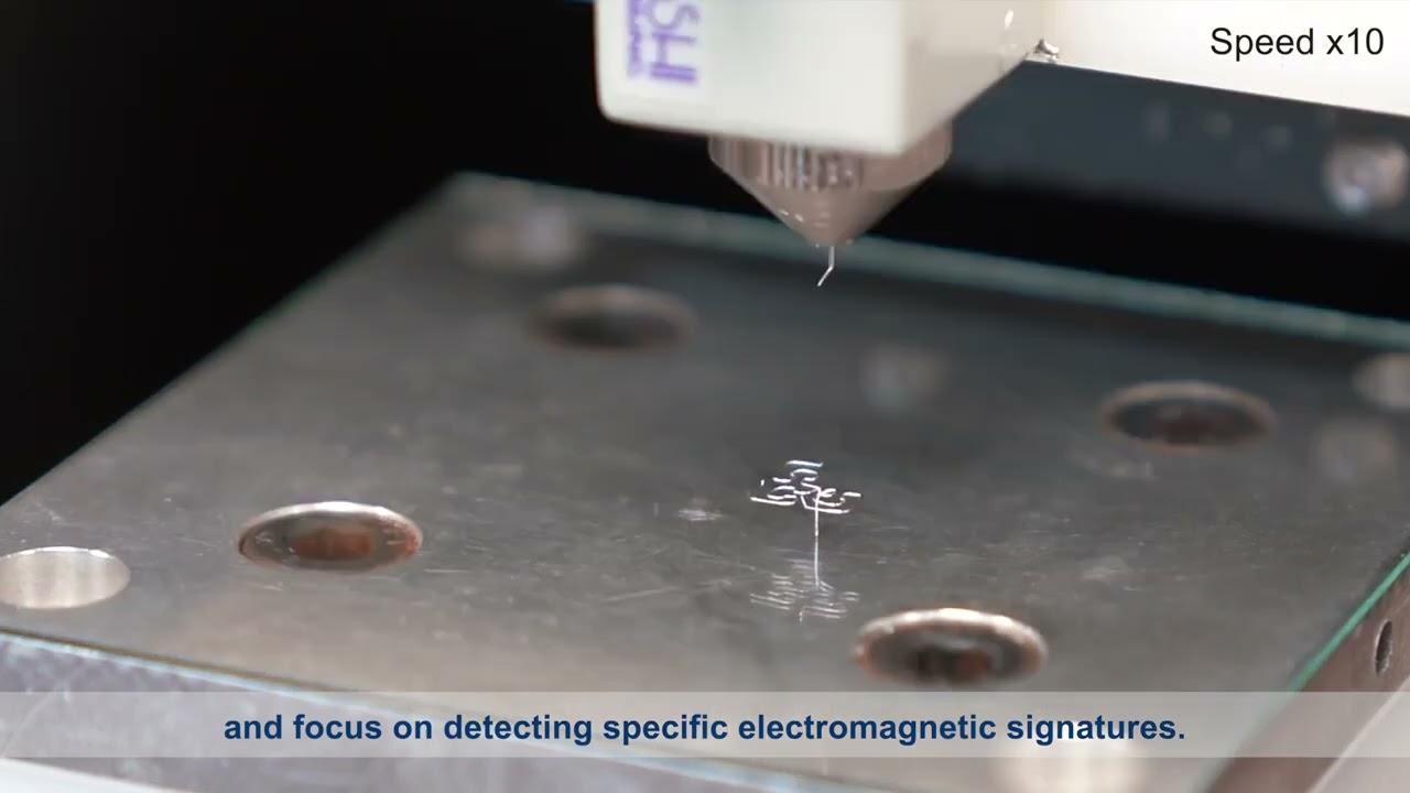
The strategy makes use of direct ink writing (DIW), which is already used to manufacture 3D circuits. The problem has all the time been that DIW makes use of supplies that aren’t good electrical conductors. That necessitates help supplies to carry every little thing collectively, limiting what you’ll be able to obtain.
CHARM3D adjustments this by incorporating Discipline’s metallic into the expertise. Discipline’s metallic is a eutectic alloy of indium, bismuth, and tin and has a reasonably low melting level for metallic. In reality, its melting level is decrease than that of the generally used supplies for hobbyist 3D printing, 62º Celsius (143.6º F). It additionally solidifies quickly, not like most composite inks usually utilized in DIW.
The mix of those traits makes Discipline’s metallic a wonderful materials for direct ink writing three-dimensional circuits. CHARM3D makes use of it to manufacture extremely advanced free-standing 3D buildings like vertical letters, cubic frameworks, and scalable helixes.

“By providing a sooner and less complicated method to 3D metallic printing as an answer for superior digital circuit manufacturing, CHARM3D holds immense promise for the industrial-scale manufacturing and widespread adoption of intricate 3D digital circuits,” Tee mentioned.
Tee’s crew additionally highlights the product’s self-healing properties. Because it has a low melting level, the mere utility of a warmth gun can restore a damaged circuit in seconds.
The engineers have already used CHARM3D to manufacture a 3D circuit for a wearable battery-free temperature sensor, antennas for wi-fi important signal monitoring, and metamaterials for electromagnetic wave manipulation. The crew believes the expertise might allow extra correct medical imaging, corresponding to microwave breast most cancers imaging to detect tumors earlier. The researchers observe that it additionally holds promise in superior safety purposes, corresponding to screening for hidden units or contraband.
Tee and his crew imagine they’ve solely begun to discover what the approach behind CHARM3D can do and are in search of alternatives to commercialize their work.